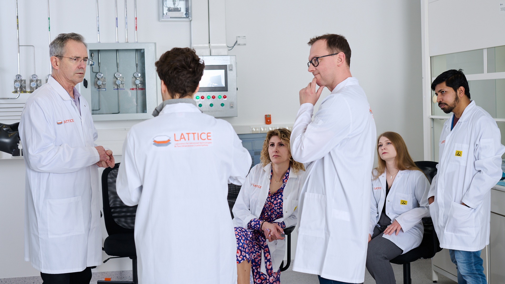
Next-generation electronics laboratory
Two-dimensional (2D) materials are a key research focus for physicists at Warsaw University of Technology (WUT). Recently, the team gained access to cutting-edge industrial-grade equipment for synthesizing 2D materials and their heterostructures. The LATTICE Laboratory (Laboratory for Advanced Technologies in Two-Dimensional Crystal Epitaxy) operates within CEZAMAT.
"The centerpiece of our lab is a metal-organic chemical vapor deposition (MOCVD) reactor," explains Jakub Sitek, PhD. "It enables semi-industrial-scale production of 2D materials. Our goal is to develop these materials for electronics –transistors, photodetectors, sensors, and optoelectronic devices."
Smaller means better
Why are 2D materials groundbreaking? The answer lies in miniaturization. Six decades ago, Intel co-founder Gordon Moore observed that transistor counts in integrated circuits double every two years. While transistor sizes shrank to keep pace with Moore’s Law, the physical limits of silicon-based technology are now being reached – even as global demand grows for energy-efficient, high-performance electronics.
2D materials offer a solution, surpassing the limitations of conventional monocrystalline silicon. "They could revolutionize electronics because, unlike silicon, they function at atomic-scale thicknesses, unlocking unprecedented miniaturization," says Sitek, PhD. "This also means lower power consumption and new functional possibilities."
In the world of 2D materials, layering is key. By stacking these materials strategically, researchers can create metamaterials with enhanced or entirely new properties.
Pushing boundaries
"The industry has invested heavily in silicon technology and won’t abandon it overnight," notes Sitek, PhD. " A transitional step might involve integrating 2D with 3D structures, but, in our opinion, it's not currently beneficial to focus on such hybrids. We’re focusing on purely 2D-based innovations, like neuromorphic computing architectures."
Globally, only a few research groups specialise in MOCVD for 2D materials – led by Penn State University in the U.S. The WUT Faculty of Physics team is Poland’s only group deeply engaged in applying this technology to electronics, aiming to compete at the highest level to match researchers from Pennsylvania.
Currently, the team is testing first-generation samples. The ultimate goal is to achieve the "gold standard" – laboratory-tested devices proving the quality and scalability of their 2D material solutions.
The LATTICE team includes. Jakub Sitek, PhD, Iwona Pasternak, PhD, Abinash Adhikari PhD (POSTDOC WUT), Alicja Kądziela, MSc, (PhD student, Preludium BIS), and Prof. Włodzimierz Strupiński. The laboratory operates under the 2D Materials Growth Group led by Prof. Mariusz Zdrojek in his research project.
The innovative platform for synthesizing 2D materials and their heterostructures for next-generation electronics was established thanks to funding from the Ministry of Education and Science, totalling PLN 9.3 million (≈$2.2M)

