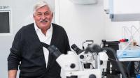
30 million złoty for terahertz technology research at WUT

Research by Prof. Wojciech Knap (the principal investigator in the project) initiated the emergence of a new field – terahertz plasmonics
The new project of the Warsaw University of Technology, "Research and Application Center for Terahertz Technologies CENTERA2", will be conducted in the laboratories of the Center for Advanced Materials and Technologies (CEZAMAT) under the leadership of Prof. Wojciech Knap and Prof. Marek Potemski.
The International Research Agendas (IRA) program enables the creation of research centers in Poland that attract outstanding scientists from all over the world. The Foundation for Polish Science has just announced the winners of this program, including the "Research and Application Center CENTERA2" project submitted by the Warsaw University of Technology.
The CENTERA2 project is a continuation of the CENTERA project, which began in 2018 in collaboration between the Warsaw University of Technology and the Institute of High Pressure Physics of the Polish Academy of Sciences.
– Thanks to the consortium, consisting of these two institutions, we were able to establish a laboratory at the Centre for Advanced Materials and Technologies CEZAMAT PW that possesses all types of terahertz spectrometry, as well as magnetic fields, cryogenic devices, and high-pressure equipment – explains Prof. Wojciech Knap.
Currently, the CENTERA laboratory enables multidisciplinary research, allowing terahertz technologies to be developed with applications in mind for the economy and industry, as well as in certain areas of everyday life.
– One of the biggest problems in the area of terahertz waves is the lack of inexpensive and efficient sources and detectors – explains Prof. Knap. – Reducing the production costs of such devices can be achieved through the development and manufacturing of innovative high-frequency (terahertz) semiconductor technologies based on silicon or gallium nitride. I believe that in Poland, we have the capability to develop this technology.
By lowering the production costs, devices could eventually be implemented, for example, on a production line, where quality control of products made from synthetic polymers could be conducted using terahertz waves.
Using terahertz waves for scanning instead of X-rays would guarantee a certain level of "safety", associated with the fact that in the case of THz, we are dealing with low ionizing energy.
– There's no removal of atoms or modification of chemical compounds here. In this way, we could eliminate devices based on harmful X-ray radiation to biological organisms – explains Prof. Knap.
In the future, terahertz waves will also be used in communication solutions, as the higher the carrier frequency, the faster the data transmission speed.
The goal of the CENTERA2 project is to create one of the best research teams in Europe at the Warsaw University of Technology, focusing on THz technologies. The project will establish four teams, focusing on the study of new phenomena in condensed matter that could be used for the detection, modulation, generation, and amplification of THz radiation, new materials based on research on quasi-particles, the development of tools for modeling new phenomena using electronic and magnetic excitations, and the development of new devices and systems for technology transfer and commercialization. This last area is particularly important, as the CENTERA2 project is primarily aimed at focusing on the practical application of terahertz waves.
Nearly thirty researchers will be employed in the project, with the work being carried out under the leadership of Prof. Wojciech Knap, who over 25 years ago began researching terahertz waves and was the first to experimentally demonstrate that plasma wave oscillations in nanostructures could reach the terahertz range, thereby initiating the emergence of a new field – terahertz plasmonics. In the CENTERA2 project, Prof. Knap serves as the principal investigator. Prof. Marek Potemski, a recognized expert in the field of physics of low-dimensional semiconductor materials, is the leader of the research team in the project.


