
What could replace silicon in electronics?
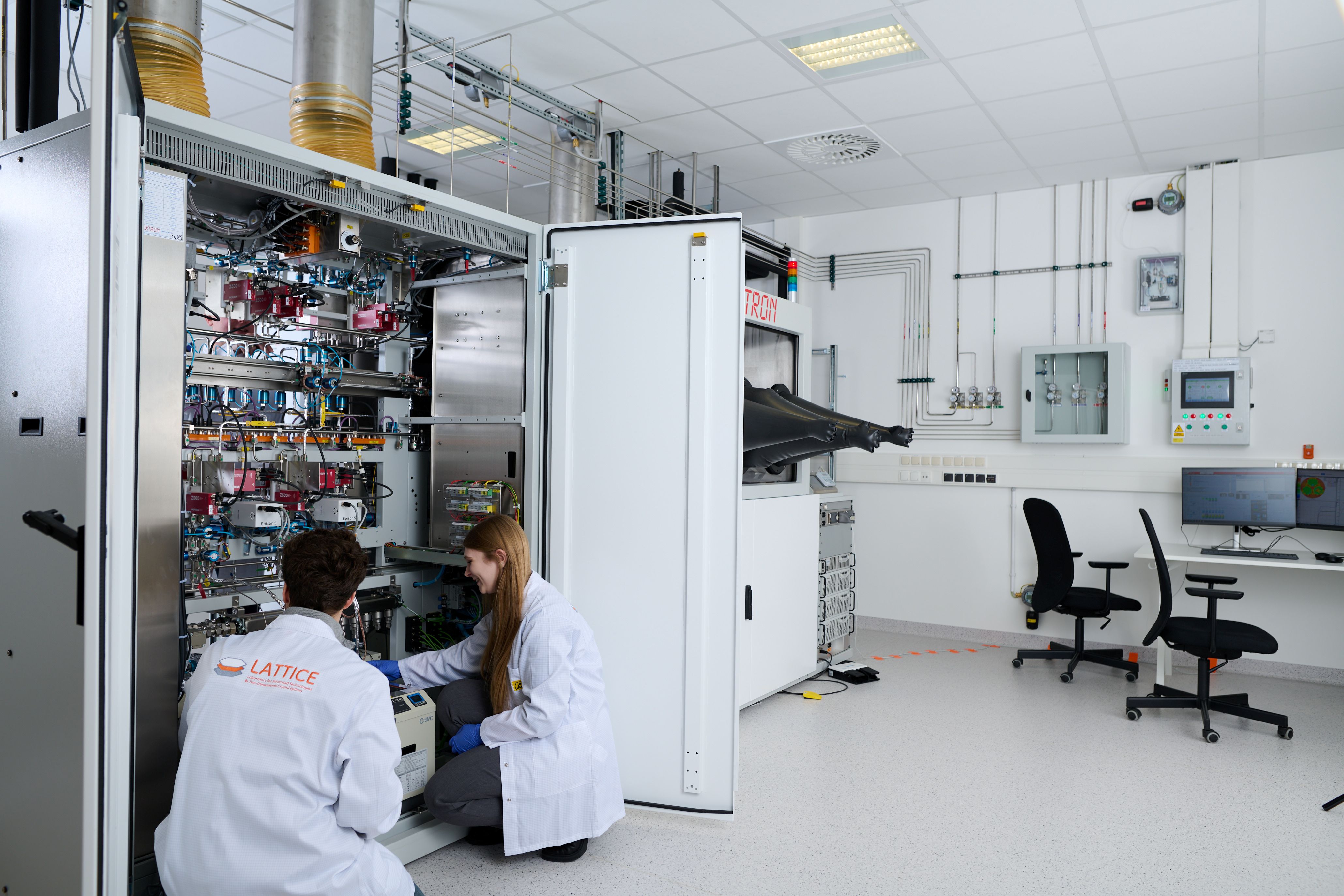
Centre for Advanced Materials and Technologies CEZAMAT
For decades, silicon has been the driving force behind the development of electronics. However, its capabilities are not limitless. Jakub Wojciech Sitek, PhD, from the Centre for Advanced Materials and Technologies CEZAMAT at the Warsaw University of Technology will lead a research project aimed at developing a solution that could support the next generation of electronic devices.
Modern electronics relies almost entirely on silicon. For several decades, engineers have successfully miniaturised electronic components such as transistors, making computers and smartphones faster and more energy-efficient. Today, however, silicon is approaching its physical limits. Further miniaturisation reduces device performance, may ultimately prevent proper operation, and leads to a significant increase in power consumption. This challenge has become particularly evident with the rapid development of artificial intelligence, which requires enormous computing power.
One of the most promising alternatives to silicon is electronics based on two-dimensional (2D) materials consisting of one or only a few atomic layers. This family includes semiconductors such as molybdenum disulfide (MoS₂) and tungsten diselenide (WSe₂). Unlike the well-known graphene, these materials possess a band gap, enabling them to function as "ultra-thin silicon"—ideal active layers for atomically thin transistors.
To build practical integrated circuits from these materials, researchers must develop reliable methods of doping them, that is, introducing a controlled number of foreign atoms to modify their electrical conductivity from n-type (electron-rich) to p-type (hole-rich). While this has been standard practice in silicon technology for decades, stable doping remains one of the greatest challenges for 2D materials. Existing approaches are either unstable or limited to small flakes obtained by mechanical exfoliation.
The project, entitled SCALED – Scalable, Controllable and Atomically Flat Epitaxy of Doped 2D Semiconductors for Post-Silicon Electronics, aims to develop a scalable, reproducible and technologically viable method for doping monolayers of MoS₂ and WSe₂ directly during growth in an industrial metal-organic chemical vapour deposition (MOCVD) reactor. The researchers will use two carefully selected dopants: rhenium (Re) to obtain n-type conductivity in MoS₂ and niobium (Nb) to achieve p-type conductivity in WSe₂. Quantum-mechanical calculations and previous experimental studies indicate that these elements are among the most promising dopants because their atoms can readily substitute the metal atoms in the crystal lattice without degrading the material's quality.
"There is no electronics without doping. In this project, my team and I will work on introducing foreign atoms into materials that are only one atom thick in a controlled and efficient way so that we can precisely tailor their electrical properties. The project is highly ambitious because it not only addresses the doping process itself but also aims to scale the technology for industrial applications. If we succeed - and I believe we will - it could revolutionise consumer electronics in the coming years," says Jakub Wojciech Sitek, PhD.
The research will consist of three main stages. First, the team will optimise the growth of high-quality, undoped MoS₂ and WSe₂ monolayers on sapphire substrates. Next, they will systematically investigate how process parameters - including temperature, pressure and precursor flow rates -affect the concentration and distribution of Re and Nb dopants using Raman and photoluminescence spectroscopy, electron microscopy and Hall-effect measurements. Finally, the researchers will fabricate field-effect transistors (FETs) directly on the grown layers and correlate their electrical performance - including carrier mobility, carrier concentration, contact resistance and on/off current ratio - with growth conditions and doping levels.
The project will produce a comprehensive "design map" for doping MoS₂:Re and WSe₂:Nb, linking MOCVD process parameters with structural and electrical properties as well as the performance of actual transistors. In the final stage, the technology will be scaled up from small 1 × 1 cm samples to full 2-inch sapphire wafers, bringing it closer to the standards required by the semiconductor industry.
Developing a stable and reproducible method for doping 2D semiconductors is one of the missing building blocks on the path towards “post-silicon” electronics. In the future, the project's results could contribute to the development of energy-efficient electronic systems for artificial intelligence, including neuromorphic computing architectures, as well as advanced sensors and photodetectors. They may also strengthen the position of Polish research institutions in the global race to develop 2D electronics.
The project SCALED – Scalable, Controllable and Atomically Flat Epitaxy of Doped 2D Semiconductors for Post-Silicon Electronics has received funding under the SONATA 21 programme.
© 1998-2026 Warsaw University of Technology
Pl. Politechniki 1, 00-661 Warsaw, Poland