2D electronics on an industrial scale?
Another important step forward in 2D materials research. Working in an international team of researchers, Jakub Sitek, PhD, from the PW Faculty of Physics, developed a new method which opens up the way to mass production of 2D materials based devices. The results of the team’s research were published in "ACS Applied Materials & Interfaces".
Dr Sitek concentrated on van der Waals heterostructures, "sandwiches" connecting various types of 2D materials, which facilitate manufacturing of advanced electronics based on 2D materials. Soon we will see them in, for example, flash memory drives, electroluminescent diodes or gas sensors.
At present most 2D materials based devices are manufactured with the exfoliation method that causes defects and pollution in layers, which limits the efficiency of electronic devices. Exfoliation does not make scaling possible, which is a huge obstacle from the industrial point of view. The challenge is thus to choose heterostructure manufacturing methods so that they ensure scalability and repeatability, and also provide the option of modifying selected parts of the substrate – all that in order to reduce the number of technological operations resulting in various defects.
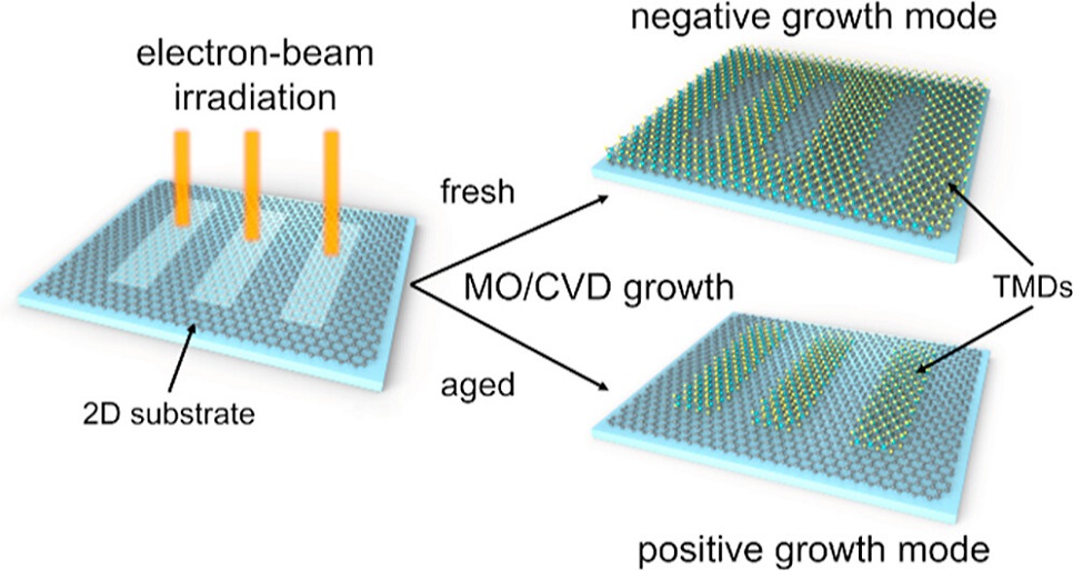
– Our team has developed a method of selective manufacturing of van der Waals heterostructures through chemical deposition from the gaseous phase with electron beam irradiation – says dr Sitek. – The process consists of irradiation of the substrate, e.g., graphene, with a very strong electron beam. Electrons modify the substrate and at the same time saturate it with an electric charge. Then on the irradiated substrate we grow another layer of 2D materials, e.g., semiconductors like wolfram sulphide WS2.
The most interesting aspect of the method is the fact that we can control the result of substrate irradiation.
– If the substrate is "aged", then in the irradiated spots another layer grows and if it is "fresh", the growth is blocked in irradiated spots, which opens up completely new possibilities for the industry – adds the PW scientist.
The method is so innovative than it was submitted for an international patent (no. PCT/PL2023/050013). Its authors are Jakub Sitek, PhD, and Karolina Czerniak-Łosiewicz, PhD – both from the group of Professor Mariusz Zdrojek. Our researchers are planning to commercialise their invention and apply for funding from the Foundation for Polish Science within the programme Proof of Concept. Their results might be of interest to the largest technological companies, such as Intel, which started work on similar methods.
The article "Selective Growth of van der Waals Heterostructures Enabled by Electron-Beam Irradiation" is available here.
The research was conducted thanks to financing from EU Graphene Flagship and PRELUDIUM NCN grants.


